

%20(00000)%20-%20Copy-min.jpg?width=1170&name=Ionic%20Contamination%20CU(00000)%20(00000)%20-%20Copy-min.jpg)
The Challenge of Cleaning Complexity
As technological applications become increasingly complex, so too do the printed circuit boards that power them. Today, PCBs are able to do more while utilizing less space through the implementation of:
- Lower component standoff heights
- Increased board density
- Stacked and complex component types
- Increased use of sensitive materials
Finding the right cleaning product for your application is critical. At ZESTRON, our high precision cleaning agents are powered by proprietary chemical technology. We deliver defluxing solutions compatible with a wide array of electronics and materials, completely tailored process solutions, and a commitment to develop industry-leading engineered chemistry through continual investment in R&D.
Be confident that your cleaning process will be optimized to stay ahead of the latest printed circuit board technology.
Causes of PCB Field Failure
There are many reasons why a board could fail in the field. The risk of failure can be mitigated by removing residue related to production and handling. Components of solder paste (resins, rosins, and fluxes) are integral to the PCB manufacturing process, but if residues from these elements are not removed after the assembly process, they can lead to common and predictable problems.
1. Electrochemical Migration (ECM)
Electrochemical Migration is “the growth of conductive metal filaments or dendrites on or through a printed board under the influence of a DC voltage bias” (IPC-TR-476A). ECM can form unintended connections on your PCB that can cause shorted-out components. Two common ECM mechanisms are:
- Conductive anodic filaments (CAF) which form when migration occurs within a PCB.
- Dendrite growth which occurs along the PCB surface producing a tree-like (dendrite) morphology.
.jpg?width=1000&name=Electr%20Photo%20(005000).jpg) Electrochemical Migration On PCB
Electrochemical Migration On PCB
2. Contamination Induced Leakage Current
Flux activators left on the board after the PCB assembly process are the most common source of leakage current on circuit assemblies. No-clean fluxes should encapsulate the activators through an inert resin layer, but due to the solder profile, heat distribution, and thermal cycling (with the added influence of copper distribution and heavy components) there may be an insufficient encapsulation of the activators. If they are present in areas of the PCB where there are high demands for surface insulation resistance, moisture in the environment could cause a leakage of current, compromising signal integrity and potentially leading to component or board failure. These areas could be close to ground conductors, voltage circuit conductors, support capacitors, between pins of oscillator contacts, or measuring bridges.
_1.jpg?width=1000&name=Current%20Leakage%20(00000)_1.jpg)
Leakage Current On PCB
3. Conformal Coating Defects
Conformal coatings are layers of material that are applied on and adhere to the PCB and its components to protect from environmental hazards. There are a wide variety of materials used as conformal coatings ranging from thick layers of silicone to nano-coatings like Parylene. The coating, when applied, will conform to the shape of everything on the surface, including any contaminants or residues leftover from the production process. Trapped contaminants can cause conformal coatings to warp, crack, or peel which re-exposes the PCB to the environmental hazards the coating layer was meant to protect against.
4 Methods for Cleaning Your PCBs
If attention is not paid to potential failure mechanisms throughout the PCB manufacturing process, long term board reliability can be compromised. Cleaning contaminants and residue from circuit assemblies at key stages is a crucial part of any reliability engineering process and serves as a proactive risk mitigation against field failure.
1. Inline Cleaning Machine
Spray-in-air inline cleaning machines are ideal when cleaning electronic assemblies with densely populated boards having low standoff components and when requiring high production throughput. The PCB are placed on an automatic conveyor belt and run through individual process steps, where cleaning, rinsing and drying are performed in separate sections of the inline machine.
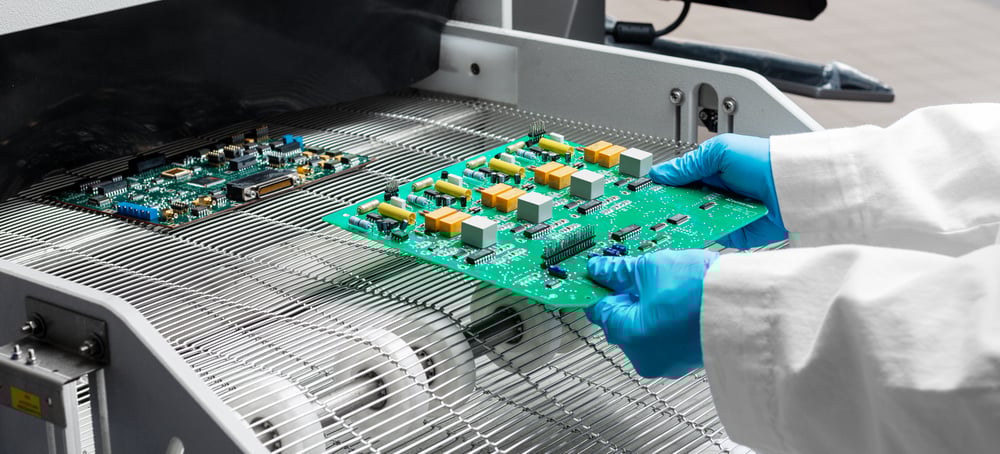
Inline Cleaning
2. Batch Cleaning Machine
The spray-in-air batch system operates using technology very similar to the technology used in a dishwasher. All process steps are executed within the same process chamber. The cleaning medium is sprayed onto the electronic assemblies through nozzle fittings on rotating spray arms. The cleaning effect is achieved primarily by the volume of cleaning medium passed over the substrates rather than the spray jet pressure like in inline processes.
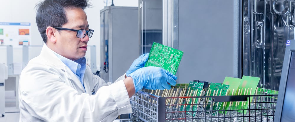
Batch Cleaning
3. Ultrasonic Cleaning Machine
Ultrasonic systems submerse the PCB in a cleaning medium that is then agitated with sound waves exceeding 20 kHz. Ultrasonic cleaning can be useful in cleaning under components and complex geometries since the sound waves are capable of reaching the populated circuit board from every angle. Many industry cleaning machines have an automatic frequency adjustment for the modulation of the ultrasound (sweep) working frequency, which prevents “hot spots” and allows material-friendly cleaning.
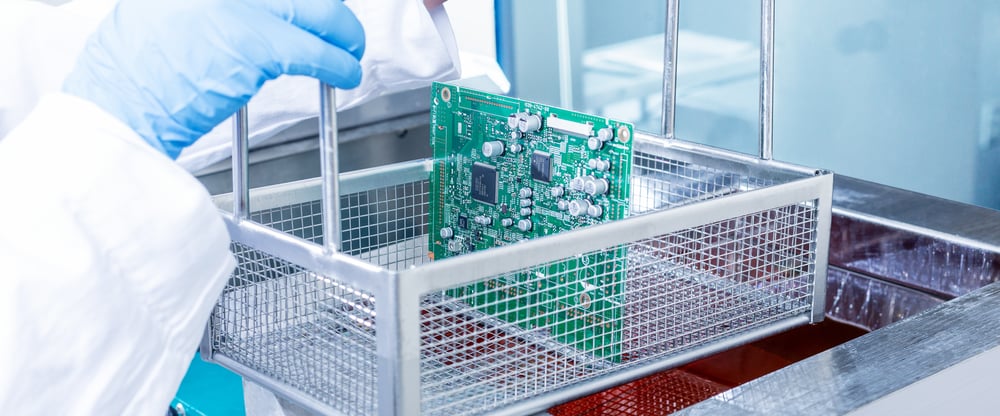
Ultrasonic Cleaning
4. Manual Cleaning
Sometimes individual PCB need to be cleaned with unique geometries and materials. In this case, nothing beats good, ol’ fashioned elbow grease. Manual cleaning requires no investment in equipment and is popular in applications where the throughput is low like building prototypes or performing electronic component rework/repair. If a facility is producing medium/high throughput, running several shifts and requires reliable and repeatable cleaning results, an automated cleaning process is recommended.
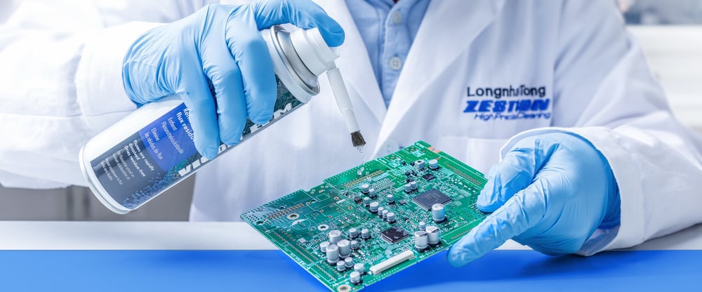
Manual PCB Cleaning
Our engineering team provides complete process optimization solutions and recommendations, offering more than just a product. ZESTRON can help you to better manage your performance, measure your results, and control your costs. ZESTRON’s Technical and Analytical Center uses industry leading equipment to conduct cleaning trials to determine the best solution for your cleaning challenges.